PCB board manufacturing process from design files to final inspection
What the PCB board manufacturing process does
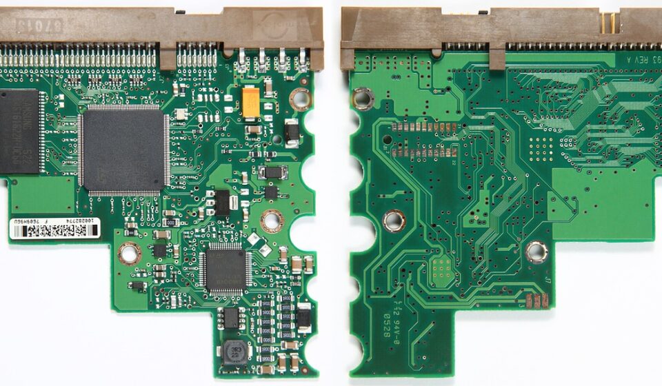
The PCB board manufacturing process turns verified design data into a bare printed circuit board ready for electronic assembly. For a typical rigid multilayer PCB, the work moves through CAM review and panel planning, inner-layer imaging, etching, automated optical inspection, lamination, drilling, desmear, copper deposition, electroplating, outer-layer imaging, solder mask, surface finish, profiling, electrical testing, and final inspection.
The exact route depends on layer count, via type, material system, board thickness, copper weight, surface finish, and reliability class. For buyers and engineers, the key point is that PCB fabrication is not a single operation. It is a controlled sequence in which early design, stackup, and tooling decisions affect many later steps. For more articles on industrial production methods, see our manufacturing processes section.
The typical process flow at a glance
Factories may organize their departments differently, but most rigid PCB fabrication lines follow the same engineering logic. A simple two-layer board may bypass inner-layer lamination steps, while HDI, metal-core, rigid-flex, or high-frequency boards require additional controls and special operations. The table below summarizes the core flow for a common rigid multilayer PCB.
| Stage | Main purpose | Key risk to control |
|---|---|---|
| CAM review and panelization | Check design data, define tooling, and arrange boards on a production panel | Missing files, incompatible stackup, insufficient clearances |
| Inner-layer imaging and etching | Create copper circuitry on internal cores | Over-etch, under-etch, shorts, opens, registration error |
| Inner-layer AOI | Inspect internal circuits before they are buried | Undetected defects that cannot be repaired after lamination |
| Lamination | Bond cores, prepreg, and copper foil into a multilayer panel | Voids, resin starvation, layer shift, thickness variation |
| Drilling and desmear | Create vias and remove resin smear from hole walls | Drill wander, rough hole walls, poor interconnect reliability |
| Electroless copper and electroplating | Build conductive copper in holes and on surfaces | Thin plating, voids, poor copper distribution |
| Outer-layer imaging and etching | Form external copper traces and pads | Line width variation, annular ring loss, surface defects |
| Solder mask, surface finish, and legend | Protect copper and prepare solderable pads | Mask misregistration, finish defects, contamination |
| Routing, electrical test, and final inspection | Separate boards, verify circuits, and inspect workmanship | Open/short circuits, burrs, edge damage, cosmetic defects |
Before fabrication starts, data quality sets the limits
A PCB factory does not begin with copper. It begins with the fabrication data package. This usually includes Gerber or IPC-2581 output, drill files, a stackup, fabrication notes, material requirements, surface finish, copper weights, impedance requirements where applicable, and acceptance criteria. CAM engineers review the package against the factory’s equipment, materials, and process windows.
This step matters because many manufacturing problems are already built into the design before the first production panel is cut. Tight trace and spacing rules, small annular rings, high aspect-ratio holes, mixed copper density, unusual materials, and poorly defined impedance targets can all reduce yield. When the design is reviewed early, the manufacturer may adjust panel orientation, add coupons, compensate artwork for etch behavior, or request clarification before release to production.
Industry references such as IPC-2221 for printed board design and IPC-6012 for rigid board performance are often used to align design expectations with fabrication capability. At the time of writing in September 2026, IPC-6012F is a current widely cited rigid-board performance specification, released in 2023, while IPC-A-600M, published in May 2025, is used for visual acceptability of printed boards. These references do not replace a purchase specification, but they help buyers and fabricators use a shared language for quality and inspection.
How copper circuitry is formed
Inner-layer imaging and etching
For multilayer boards, production often starts with thin copper-clad cores. Each core is cleaned, coated with photosensitive resist, exposed with the circuit image, and developed so that only selected copper areas remain protected. Etching removes the unwanted copper. After the resist is stripped, the intended inner-layer traces, planes, pads, and clearances remain.
Because these layers will later be buried inside the board, factories inspect them before lamination using automated optical inspection. AOI compares the manufactured copper pattern with the digital reference and flags opens, shorts, nicks, mouse bites, excess copper, or spacing violations. Repair options are limited and controlled. For high-reliability work, the usual goal is to identify and remove defective panels before more cost and process time are added.
Lamination builds the multilayer structure
Lamination turns individual circuit layers into one solid panel. Cores, prepreg sheets, and copper foil are stacked in a controlled sequence, aligned with tooling pins or optical registration systems, and pressed under heat and pressure. The resin in the prepreg flows and cures, bonding the structure and creating insulation between copper layers.
This is where stackup discipline becomes visible. Resin content, glass style, copper distribution, pressure cycle, and material compatibility influence final thickness, flatness, dielectric spacing, and impedance. Heavy copper or unbalanced copper layouts can create local resin-flow problems. High-speed and RF designs add another level of sensitivity because dielectric properties and thickness tolerance can affect signal behavior.
Drilling, desmear, and plating create interconnection
Modern PCBs rely on vias to connect layers. Mechanical drilling is common for through holes and many buried structures. Laser drilling is used for microvias and HDI designs. The drilling program must match the stackup, finished hole size, plating allowance, and registration capability. Small holes in thick boards increase aspect ratio, which makes cleaning and plating more difficult.
After drilling, the hole walls are not ready for reliable plating. Resin smear caused by the drill must be removed so the internal copper layers are cleanly exposed. Desmear and surface activation prepare the hole wall for electroless copper, a chemical deposition step that creates a thin conductive layer through the holes and across the panel surface. Electrolytic copper plating then builds the required copper thickness.
This sequence is central to reliability. A board may look acceptable from the outside yet fail because of plating voids, thin copper in the barrel, poor adhesion, or microcracks around vias. For this reason, process control often includes cross-section analysis on production coupons, plating thickness checks, solderability evaluation, and electrical testing. IPC-6012F expanded attention to issues such as microvia reliability, copper wrap plating, dielectric spacing, and microsection evaluation, reflecting the higher density and reliability demands of current rigid-board fabrication.
Outer layers, solder mask, and surface finish complete the board
Once the conductive holes are established, the outer copper pattern is produced. The panel is coated with photoresist, imaged, developed, plated where required, and etched so that outside traces, pads, annular rings, and copper features match the design. Outer layers are sensitive because they must meet both electrical requirements and assembly needs.
Solder mask is applied after copper patterning. The mask protects copper from oxidation and solder bridging while leaving component pads exposed. Liquid photoimageable solder mask is common in commercial production because it can be applied, exposed, developed, and cured with fine registration. Poor mask alignment can reduce solderable area or expose copper where it should remain protected. See also: buying guides.
The exposed pads then receive a surface finish. Common options include HASL, lead-free HASL, ENIG, immersion silver, immersion tin, OSP, and other specialized finishes. The choice should be based on assembly method, shelf life, pad geometry, wire bonding or press-fit requirements if any, cost, and reliability expectations. Fine-pitch surface-mount assemblies, for example, often need flatter finishes than traditional through-hole boards. High-reliability products may also require tighter controls on finish thickness and contamination.
Legend printing, also called silkscreen, adds reference designators, polarity marks, logos, and handling information. It is not electrically functional, but it supports assembly, inspection, service, and traceability. Finally, the panel is routed, scored, or punched to create the finished board outline. Edge plating, castellations, controlled-depth routing, and tight mechanical tolerances may add further process controls.
Inspection, standards, and environmental controls
Quality control is not only a final gate. A robust PCB board manufacturing process checks the product at multiple points, including incoming laminate verification, inner-layer AOI, post-lamination registration, drill quality, plating thickness, solder mask adhesion, surface finish condition, dimensional accuracy, electrical continuity, and final visual workmanship. Bare-board electrical testing verifies that required nets are connected and isolated from other nets. Flying-probe testing is common for prototypes and small batches, while bed-of-nails fixtures may be used for higher volumes.
Visual acceptance is often aligned with IPC-A-600, while performance requirements for rigid printed boards are commonly aligned with IPC-6012. Buyers should specify the required class, test requirements, coupons, certificates, and any application-specific addenda instead of assuming that every supplier interprets quality in the same way. Automotive, medical, aerospace, and defense boards typically require more explicit documentation than consumer or general industrial boards.
Environmental control is also part of fabrication. PCB factories use chemical cleaning, etching, plating, developing, stripping, and rinsing operations, which can generate copper-bearing wastewater, spent solutions, sludge, and rinse streams. The U.S. EPA’s Metal Finishing Effluent Guidelines under 40 CFR Part 433 identify printed circuit board manufacture among covered operations, with related controls for process wastewater. In practice, responsible factories manage chemical segregation, metal recovery, wastewater treatment, sludge handling, and documentation as part of production, not as an afterthought.
Design choices that affect yield and cost
The most cost-effective PCB is usually not the simplest-looking one. It is the design that fits a stable process window. Engineers can improve manufacturability by discussing stackup, materials, via structures, copper balance, impedance, and inspection needs before release. Several practical rules are especially important.
- Use realistic trace and spacing rules. Avoid choosing the smallest capability unless the design truly needs it.
- Control via aspect ratio. Thick boards with very small drilled holes are harder to plate reliably.
- Balance copper distribution. Large copper imbalance can affect lamination, etching, and flatness.
- Specify surface finish by assembly need. Do not choose a finish only because it is familiar.
- Define acceptance criteria clearly. Include IPC class, test requirements, coupons, impedance tolerance, and special inspection needs.
- Keep fabrication notes consistent. Conflicting drawings, stackups, and Gerber data create delays and risk.
Good design for manufacturability does not mean reducing performance. It means choosing structures that the selected factory can build repeatedly, inspect effectively, and document clearly. That is where cost, yield, and reliability meet.
Frequently asked questions
Is PCB manufacturing the same as PCB assembly?
No. PCB manufacturing usually refers to making the bare board: laminate, copper circuits, vias, solder mask, surface finish, and final board outline. PCB assembly, or PCBA, is the later process of adding components by solder paste printing, pick-and-place, reflow soldering, wave soldering, selective soldering, inspection, and functional testing.
Which step is most critical in PCB fabrication?
There is no single universal answer. For multilayer boards, lamination, drilling, desmear, and plating are especially critical because they determine layer alignment and via reliability. For fine-line boards, imaging and etching control yield. For assembly-sensitive designs, solder mask registration and surface finish quality may be decisive.
Why do manufacturers ask for stackup approval?
The stackup defines layer order, dielectric thickness, copper weight, material type, and sometimes impedance targets. It affects thickness, signal performance, drilling, lamination, and cost. Approval helps prevent misunderstandings before the board enters production.
What files are normally needed for PCB production?
A typical package includes copper layer data, solder mask layers, legend layers, drill files, board outline, stackup, fabrication drawing, material requirements, surface finish, copper thickness, controlled impedance requirements if used, and acceptance criteria. More complex boards may require coupon drawings, special notes, or customer-specific test requirements.
How can buyers reduce PCB manufacturing risk?
Buyers can reduce risk by using clear fabrication notes, avoiding unnecessary extreme tolerances, confirming the supplier’s process capability, specifying standards and inspection requirements, and resolving DFM questions before release. Early communication is usually cheaper than correcting problems after panels have already been built.


