PCB manufacturing and assembly process explained for engineers and buyers
What PCB manufacturing and assembly includes
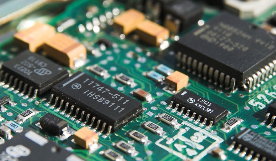
PCB manufacturing and assembly is the connected workflow that turns an electronic design into a working circuit board. Manufacturing creates the bare board through stackup preparation, imaging, etching, lamination, drilling, plating, solder mask, surface finish, profiling and bare-board test. Assembly then attaches components by SMT, through-hole or mixed technology and verifies solder joints and electrical behavior.
For engineers and sourcing teams, the decision is not only who can build the board. The more important question is whether design files, materials, soldering processes and acceptance criteria are aligned before release. Reliable PCBA work starts with design for manufacturability, clear fabrication and assembly notes, and test expectations tied to recognized standards rather than informal visual judgment. For related production topics, see our manufacturing processes section.
How bare PCB fabrication turns data into a board
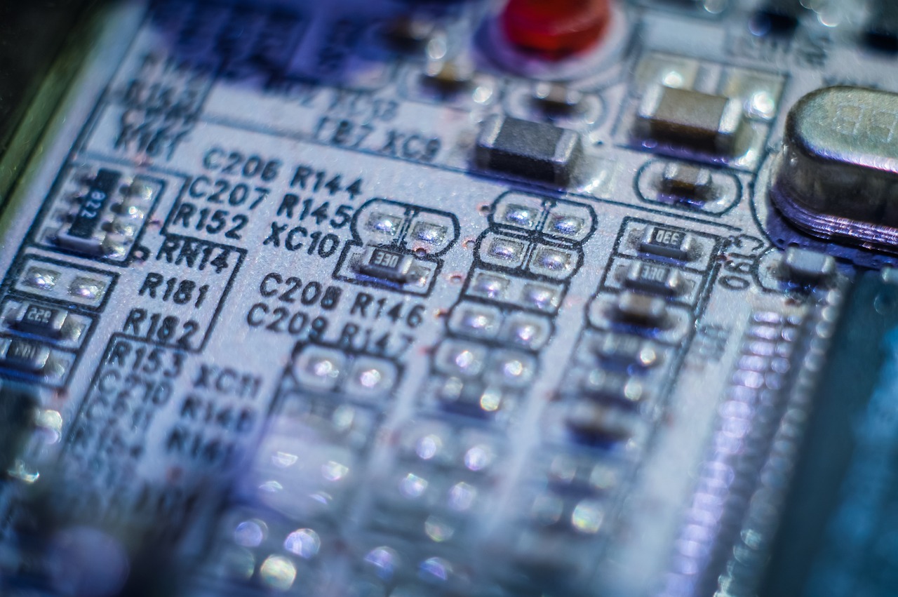
The fabrication stage starts before copper is etched. A board shop reviews the CAD output, Gerber or ODB++ data, drill files, netlist, stackup, material callouts, copper weights, controlled impedance requirements, solder mask color, silkscreen, surface finish and final dimensions. This review is often called DFM, but it should be treated as an engineering gate rather than a courtesy check. The purpose is to identify conflicts between the design intent and the fabricator’s actual process window.
Design data and stackup review
A multilayer board depends on a controlled stackup. Layer count, dielectric thickness, copper thickness and reference planes influence impedance, thermal behavior, warpage risk and manufacturability. IPC-2221C, listed by IPC as a generic printed board design standard with a December 2023 revision, is commonly referenced for broad design requirements, while sectional standards cover more specific board types. The practical takeaway is straightforward: do not release a layout until the board shop has confirmed the stackup, tolerances and impedance coupons needed for verification.
Core fabrication sequence
Equipment and chemistry vary by supplier, but a typical rigid multilayer PCB follows a recognizable sequence. Inner layers are imaged and etched, then inspected before lamination. The laminated panel is drilled, desmeared, plated and patterned on the outer layers. Additional etching defines the final copper circuitry. Solder mask protects conductors and defines exposed pads. Legend printing, surface finish, electrical test, profiling and final inspection complete the bare board.
The surface finish is not a cosmetic choice. HASL, lead-free HASL, ENIG, immersion silver, immersion tin and OSP each affect solderability, planarity, shelf life, cost and compatibility with fine-pitch packages. Assemblies with fine-pitch BGAs or dense QFNs, for example, usually need a flatter finish than basic through-hole boards. If the product must meet lead-free or regional hazardous-substance requirements, the finish also has to match the compliance documentation.
Why fabrication errors are expensive later
Fabrication problems often remain hidden until assembly or field use. Misregistration can reduce annular ring, weak plating can affect vias, poor solder mask registration can expose copper, and an unsuitable surface finish can create solderability problems. IPC announced IPC-6012F on October 18, 2023 as a qualification and performance specification for rigid printed boards, with expanded attention to areas such as cavities, copper wrap plating, solderability testing, microsection evaluation, dielectric spacing and microvia reliability. Those topics show why bare-board quality is not only a visual issue; it is also a structural and reliability issue.
How PCB assembly builds the working PCBA
PCB assembly, often abbreviated as PCBA, begins when the approved bare board, bill of materials and assembly documentation reach the production line. For high-volume electronics, surface mount technology is usually the main process because automated placement can handle small passive components, ICs and dense layouts efficiently. Through-hole technology remains important for connectors, transformers, high-mechanical-stress parts and some power components.
SMT assembly flow
The SMT process usually starts with solder paste printing through a stencil. Paste volume and aperture design matter: too much paste can cause bridging, while too little paste can create opens or weak joints. After paste inspection, pick-and-place machines position components onto the pads. The loaded board then passes through a reflow oven, where the profile must heat the assembly enough to form reliable solder joints without overheating components or the laminate.
IPC’s public release notice for J-STD-001J and IPC-A-610J, dated April 8, 2024, describes J-STD-001J as covering soldered electrical and electronic assembly requirements and IPC-A-610J as a post-assembly acceptability standard. IPC also notes that the two documents are often used together. In manufacturing terms, one guides process and workmanship requirements; the other helps judge whether the finished assembly is acceptable.
Through-hole and mixed assembly
Through-hole parts may be assembled by wave soldering, selective soldering or hand soldering. Wave soldering can be efficient when many through-hole leads are present and the board can tolerate the thermal exposure. Selective soldering is useful when only certain areas need solder and nearby SMT components must be protected. Hand soldering remains necessary for prototypes, rework and some specialized components, but it requires controlled methods and operator skill to avoid inconsistent joints.
Mixed-technology boards require more planning than either pure SMT or pure through-hole designs. Component height, pallet access, thermal shadowing and bottom-side parts all affect the sequence. A design that looks efficient in CAD can become slow and costly if connectors block solder nozzles or if heavy components require manual support during soldering.
Inspection, testing and standards that matter
Quality control in PCB manufacturing and assembly should combine process checks, visual inspection and electrical verification. No single inspection method catches every defect. Automated optical inspection can identify missing parts, polarity errors, skew, tombstoning and many visible solder defects. X-ray inspection is useful for hidden joints under BGAs, QFNs and other bottom-terminated components. In-circuit testing checks component placement and basic electrical values where test access is available. Functional testing verifies that the assembled board performs its intended operation.
| Area | Common risk | Useful control point | Relevant standard or source type |
|---|---|---|---|
| Board design | Insufficient clearance, poor stackup or hard-to-build features | DFM review before release | IPC-2221C and related design standards |
| Bare board fabrication | Weak vias, registration issues or solderability defects | Microsection, coupons, electrical test and acceptance inspection | IPC-6012F and IPC-A-600M |
| Soldering process | Opens, bridges, voiding or heat damage | Stencil control, reflow profiling and process documentation | IPC J-STD-001J and IPC-7530B |
| Assembly acceptance | Unclear judgment of solder joints or component condition | Class-based inspection criteria agreed before production | IPC-A-610J |
| Automated inspection | False calls or missed process drift | AOI program validation and feedback to process control | IPC-9716 and IPC-9716A |
Standards should not be added to a purchase order as generic decoration. A consumer accessory, industrial controller, medical device and aerospace module may require different acceptance classes, documentation depth, traceability and addenda. The buyer should specify the expected IPC class, any customer-specific workmanship requirements, whether lead-free solder is required, which test records must be delivered and how nonconforming product will be dispositioned.
Design choices that drive cost and reliability
Many PCB cost problems are designed in before a quote is requested. Layer count is an obvious driver, but it is not the only one. Very fine trace and space, small mechanical holes, high aspect ratio vias, blind and buried vias, via-in-pad, tight impedance tolerance, unusual materials, controlled depth routing and special finishes can all increase cost or lead time. These features may be necessary, but each should have an electrical, thermal or mechanical reason. See also: buying guides.
Component selection can be just as important. Fine-pitch packages save board area but reduce assembly tolerance. Bottom-terminated components improve electrical and thermal performance but may require X-ray inspection. Large connectors and heavy inductors need attention to mechanical support. Components with poor availability can delay an otherwise simple assembly. A BOM should therefore be checked for lifecycle status, packaging format, moisture sensitivity, alternates and compliance documentation before production release.
Lead-free assembly adds another layer of process control. EU RoHS rules restrict ten hazardous substances in electrical and electronic equipment unless an exclusion or exemption applies, including lead, mercury, cadmium, hexavalent chromium, PBB, PBDE and four phthalates. For PCB assembly, this affects solder alloy, component termination finish, board finish and supplier declarations. Older data from the U.S. Environmental Protection Agency also noted that lead-free assembly can require higher process temperatures, making laminate parameters such as Tg, Td and CTE important when selecting materials.
A practical handoff checklist before production
A strong handoff package reduces engineering questions, quotation errors and line stoppages. It also gives the fabricator and assembler a clear basis for acceptance. Before releasing a PCB manufacturing and assembly package, verify the following items:
- Approved schematic, PCB layout and revision-controlled fabrication outputs.
- Complete BOM with manufacturer part numbers, approved alternates, quantities and do-not-populate markings.
- Fabrication drawing with board thickness, copper weight, finish, solder mask, legend, tolerances and panel requirements.
- Assembly drawing showing polarity, orientation, special handling notes and any manual operations.
- Defined IPC class, solder alloy, cleanliness requirement and conformal coating requirement if applicable.
- Test strategy, including bare-board electrical test, AOI, X-ray, ICT, flying probe or functional test.
- Programming files, fixture requirements and acceptance limits for powered testing.
- Packaging, ESD, moisture-sensitive-device handling and labeling requirements.
- Change-control rules for substitute parts, process changes and engineering deviations.
For prototypes, the handoff can be lighter, but it should not be vague. Prototype builds are where DFM feedback is most valuable. If a supplier changes pad openings, panelization, solder paste apertures or component substitutions, those changes should be captured before the design moves to pilot or volume production.
How to evaluate a PCB manufacturing and assembly supplier
Supplier evaluation should match the product risk. A simple two-layer sensor board does not need the same audit depth as a high-density, safety-critical assembly. Still, several questions are useful for most projects: What board classes and materials does the shop build regularly? Which assembly technologies are in-house, and which are outsourced? How are stencil design, reflow profiles and AOI programs validated? What inspection records are available? How are component shortages and substitutions handled?
It is also important to separate stated capability from routine yield. A supplier may advertise very fine features, microvias or complex mixed assembly, but the better question is whether those features are stable at the required volume, documentation level and delivery schedule. For production work, repeatability is more valuable than a one-time capability claim.
The clearest buying strategy is to involve the fabricator and assembler before design lock. Early input can prevent avoidable cost from unnecessary HDI layers, inaccessible test points, soldering conflicts or over-tight mechanical tolerances. Once the board is released, the supplier can only quote the difficulty that remains.
Frequently asked questions
What is the difference between a PCB and a PCBA?
A PCB is the bare printed circuit board, including insulating substrate, copper circuitry, solder mask, surface finish and mechanical shape. A PCBA is the assembled board after electronic components have been soldered and inspected. Manufacturing creates the PCB; assembly creates the PCBA.
Which files are needed for PCB manufacturing and assembly?
At minimum, the supplier needs fabrication outputs, drill data, a fabrication drawing, BOM, pick-and-place data and an assembly drawing. For controlled products, the package may also include impedance requirements, test procedures, programming files, approved vendor lists, coating notes and traceability requirements.
Is SMT always better than through-hole assembly?
No. SMT is efficient for compact, automated assembly and dense electronics, but through-hole parts can be better for high mechanical load, some power applications and connectors that experience repeated insertion force. Many industrial boards use both technologies.
Which IPC standard defines PCB assembly quality?
There is not one single standard for every decision. IPC J-STD-001J is commonly used for soldered assembly requirements, while IPC-A-610J is used for finished assembly acceptability. Bare board fabrication and inspection may involve IPC-6012F, IPC-A-600M and related design standards, depending on the product and contract.
How can teams reduce PCB assembly cost without reducing reliability?
Start with DFM and DFT before layout release. Avoid unnecessary layer count, excessive tolerances, hard-to-source parts and inaccessible test points. Use standard package sizes when possible, confirm the stackup early, and define inspection requirements clearly so the supplier does not price uncertainty into the quote.