Semiconductor chip manufacturing process from wafer fabrication to advanced packaging
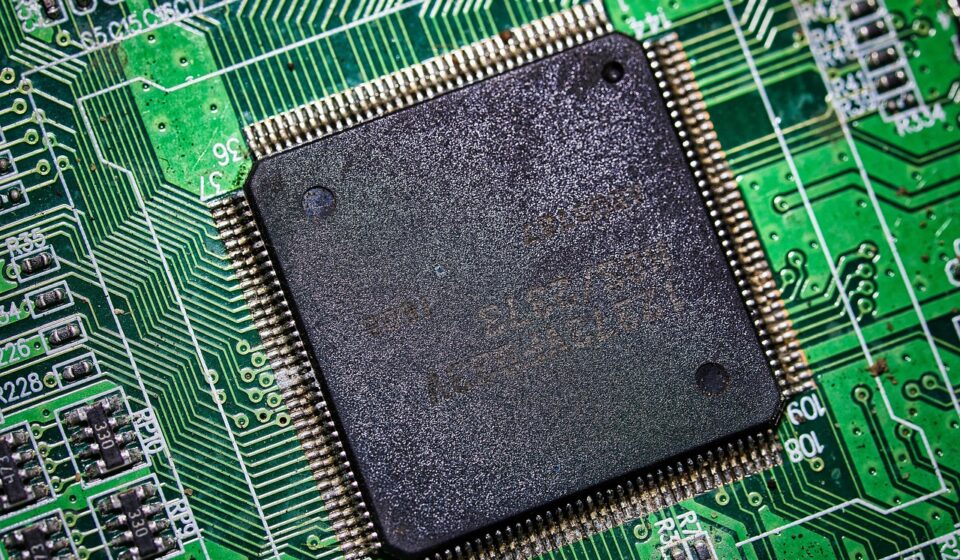
A practical view of the semiconductor chip manufacturing process
The semiconductor chip manufacturing process turns a polished silicon wafer into many working integrated circuits through repeated cycles of film deposition, lithography, etching, doping, cleaning, inspection and electrical testing. After wafer fabrication, known-good dies are separated, packaged, connected to the outside world and tested again. The basic flow is straightforward to describe, but in production it becomes a tightly controlled manufacturing system with hundreds or thousands of operations spread over several weeks.
For readers who follow precision manufacturing processes, chipmaking is a useful benchmark. It brings together motion control, vacuum engineering, chemistry, thermal stability, contamination control and statistical process control at extremely small dimensions. A chip fab is not just a clean factory; it is a yield-learning system where a microscopic defect can affect cost, performance and supply.
| Phase | Main purpose | Typical operations | Main manufacturing risk |
|---|---|---|---|
| Design and mask preparation | Convert circuit design into manufacturable patterns | EDA layout, process design kit checks, mask writing | Design rule errors, mask defects, process mismatch |
| Wafer preparation | Create a flat, clean silicon starting surface | Crystal growth, slicing, polishing, cleaning | Particles, crystal defects, surface non-uniformity |
| Front-end wafer fabrication | Build transistors and other device structures | Deposition, lithography, etch, ion implantation, anneal, CMP | Overlay error, line roughness, contamination, yield loss |
| Back-end interconnect | Connect devices into circuits | Dielectric deposition, via formation, metal fill, planarization | Resistance, capacitance, voids, electromigration |
| Assembly and test | Turn finished dies into usable components | Wafer sort, dicing, bonding, packaging, burn-in and final test | Package stress, thermal limits, connection defects |
Before a wafer enters production
Chip manufacturing starts before any wafer reaches a production tool. Engineers design the circuit, verify the logic and physical layout, and check the design against the foundry process design kit. The process design kit defines what the fab can reliably print and build, including minimum spaces, metal rules, allowed transistor options, density limits, thermal assumptions and many other constraints.
Once a design is ready, its patterns are converted into photomasks or reticles. These precision glass templates are used by lithography scanners to transfer circuit features onto coated wafers. In advanced logic, a single product can require many masks because the chip is built as a stack of layers rather than carved from one solid block. Each mask layer must align with previous and future layers, which makes overlay control one of the central challenges in semiconductor manufacturing.
This design-to-mask stage is also why process technology is not only a factory issue. A new node needs equipment, materials, design rules, device models, reliability data and software ecosystem support. If any of those pieces are immature, a process that looks advanced on paper may still be difficult to use at commercial yield.
Preparing the silicon wafer
Most mainstream integrated circuits begin with a highly purified single-crystal silicon wafer. Silicon is grown into an ingot, sliced into thin wafers, flattened, polished and cleaned. The wafer surface must be extremely smooth because later device structures are measured in nanometers. Even a small surface variation can create problems when a scanner focuses light, when a film is deposited or when a pattern is etched.
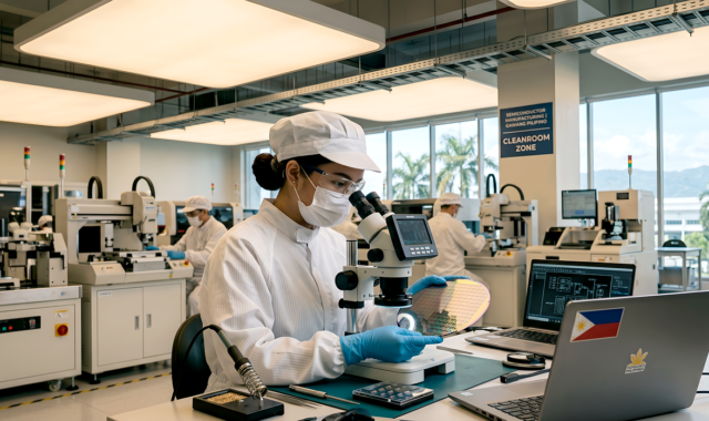
Wafers are typically handled in sealed carriers and moved through automated transport systems to reduce human contact. Cleanroom classification, airflow, chemical purity, temperature stability and vibration control all matter. Unlike many mechanical manufacturing environments, the target is not only dimensional accuracy at the workpiece level; it is also molecular and particulate cleanliness at high production scale.
Wafer preparation may include initial oxidation or other surface conditioning steps. From there, the wafer enters a repeated build-pattern-remove-modify sequence. The important point for non-specialists is that chipmaking is cumulative. A problem introduced early may be buried under later layers, making root-cause analysis difficult unless in-line inspection catches it quickly.
Building devices layer by layer in the fab
Wafer fabrication is often divided into front-end-of-line, middle-of-line and back-end-of-line work. Front-end steps form transistors and isolation structures. Middle steps create local contacts. Back-end steps build the metal wiring stack that connects billions of devices into functioning circuits. The same broad operation categories repeat many times, but the materials, dimensions and tolerances change from layer to layer.
Deposition and oxidation create controlled films
Deposition adds material to the wafer. Equipment suppliers such as Applied Materials and Lam Research describe common methods including physical vapor deposition, chemical vapor deposition and atomic layer deposition. These processes can form conductors, insulators, barriers, liners, hard masks and other functional films. Atomic layer deposition is especially important where conformal coverage and angstrom-scale control are required.
Oxidation and epitaxy are also used when the process needs a specific silicon-based layer or a crystal-quality film. The manufacturing challenge is not simply to deposit material. The film must have the specified thickness, stress, purity, uniformity and interface quality across the entire wafer and from wafer to wafer.
Lithography transfers the pattern
Lithography is the patterning step most people associate with chip manufacturing. A wafer is coated with photoresist, aligned under a mask, exposed to light and developed so selected areas remain protected while others are opened for etching, implantation or deposition. Deep ultraviolet lithography remains important across many layers and nodes. Extreme ultraviolet lithography, using 13.5 nm light, is used for some of the most intricate layers in leading-edge logic and memory.
ASML describes EUV as a technology for printing the most complex layers, while other layers continue to use DUV systems. This distinction matters because an advanced chip is not made by one tool type. It is made by integrating multiple lithography approaches with resist chemistry, mask technology, metrology, cleaning and etch transfer. Better pattern resolution is valuable only if it can be repeated at production throughput and acceptable defect levels.
Etching removes material with selectivity
Etching removes exposed material after lithography defines where removal should occur. Wet etching uses liquid chemistry, while dry plasma etching can create more directional features. Lam Research describes reactive ion etching as a process that activates the wafer surface with charged particles to remove material and form precise structures. In advanced devices, etch must distinguish between materials that may be only a few nanometers apart.
Etch performance is judged by selectivity, profile, uniformity, damage, residue and repeatability. If the etch is too aggressive, it can damage underlying features. If it is too weak or non-uniform, later steps may fail. For that reason, etch, deposition and lithography are not isolated modules. They are integrated as a process stack.
Doping, annealing, planarization and cleaning complete each cycle
Doping modifies the electrical behavior of silicon by introducing controlled impurities. Ion implantation is widely used because it can place dopants with controlled dose and depth. Thermal annealing then repairs crystal damage and activates dopants. The thermal budget must be managed carefully because excessive heat can move dopants or degrade structures that have already been formed.
Chemical mechanical planarization, often shortened to CMP, flattens the wafer after uneven layers build up. Without planarization, later lithography would struggle to focus accurately and metal interconnect layers would become less reliable. Cleaning steps remove residues, particles and unwanted films throughout the flow. These steps may look secondary compared with lithography, but they are essential to yield.
Inspection, metrology and yield learning
Modern fabs inspect and measure wafers throughout production. NIST has emphasized that metrology is central to semiconductor manufacturing because process control, quality and performance depend on measurement. Critical dimensions, film thickness, overlay, defect density, wafer shape, electrical parameters and contamination levels all need monitoring. See also: buying guides.
The reason is practical: waiting until final test would be too late. A wafer may spend weeks in fabrication. If a drift in one deposition chamber or etch recipe is discovered only after final electrical failure, many lots may already be affected. In-line metrology shortens the feedback loop and helps engineers decide whether to continue, rework, hold or scrap wafers.
Yield is the percentage of usable dies produced from a wafer, but it is also a learning metric. New processes usually begin with lower yield and improve as defect sources are found and controlled. The learning curve depends on equipment stability, material quality, design-process interaction, fab discipline and the ability to detect rare defects. This is one reason semiconductor manufacturing capacity cannot be added as quickly as simpler assembly capacity. A fab must qualify tools, recipes, suppliers, automation and quality systems before high-volume production is stable.
Packaging and final test are now part of process strategy
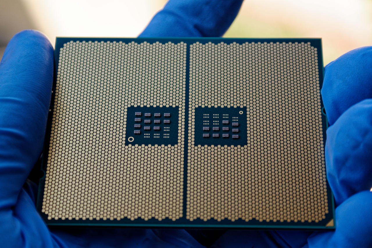
After wafer fabrication, dies are electrically tested on the wafer. Good dies are separated by dicing and assembled into packages. Traditional packaging protects the die, provides electrical connections, helps remove heat and creates a form factor that can be mounted on a circuit board. Depending on the product, the package may involve wire bonding, flip-chip bonding, underfill, substrates, lids and thermal interface materials.
For many advanced processors, packaging has become a major performance lever rather than a back-end commodity step. SEMI describes heterogeneous integration as combining separately manufactured components into a higher-level assembly with improved functionality or operating characteristics. That shift is visible in chiplet designs, 2.5D interposers, 3D stacking and high-bandwidth memory integration.
Advanced packaging changes manufacturing priorities. Interconnect density between dies, warpage control, thermal paths, substrate capacity, known-good-die strategy and package-level test can determine product cost and performance. A design may use the most advanced logic node for compute chiplets, a mature node for I/O, and specialized memory stacks in the same package. In that sense, the semiconductor chip manufacturing process now extends beyond a single monolithic die.
What is changing in advanced process nodes
Advanced process nodes are changing because traditional two-dimensional scaling has become harder. Node names such as 5 nm, 3 nm or 2 nm should be read as technology generations rather than direct measurements of one physical feature. The manufacturing difficulty comes from tighter patterning, more complex transistor structures, narrower process windows and increasing interconnect limits.
TSMC states in its public technology information that its N2 technology started volume production in the fourth quarter of 2025 and uses first-generation nanosheet transistor technology. Nanosheet and other gate-all-around transistor approaches improve electrostatic control compared with earlier planar and FinFET structures, but they also increase process integration complexity. The transistor is no longer only a smaller version of the previous structure; it can require new channel formation, selective deposition and more demanding etch steps.
Lithography is also evolving. ASML describes High-NA EUV as the next EUV generation, with a higher numerical aperture intended to support smaller features and reduce some multi-patterning complexity. On September 7, 2026, Intel Foundry and ASML reported progress in bringing High-NA EUV into production use, including more than one million wafers processed across certification, research and development, and select volume-production layers. That does not mean every chip layer moves to High-NA EUV immediately. It shows how leading-edge manufacturing adopts new tools selectively, layer by layer, while comparing cost, yield, throughput and design flexibility.
Backside power delivery is another important direction. By moving some power routing to the back side of the wafer, manufacturers aim to reduce front-side congestion and improve performance. The trade-off is a more complex process flow involving wafer thinning, alignment and additional integration risk. Together with advanced packaging, these technologies show that future gains come from system-level manufacturing choices, not only from shrinking one transistor dimension.
Key takeaways for manufacturing readers
- The semiconductor chip manufacturing process is a repeated sequence of additive, subtractive, modifying and measuring steps, not a single linear operation.
- Lithography defines patterns, but deposition, etch, clean, CMP and metrology determine whether those patterns become reliable devices.
- Yield is the main economic measure because microscopic defects can turn expensive wafer area into unusable die.
- Advanced nodes rely on technology integration: EUV, nanosheet transistors, new materials, backside power and advanced packaging must work together.
- Mature nodes remain important for analog, power, automotive, RF, sensors and many industrial applications, so not all semiconductor manufacturing is about the smallest node.
Frequently asked questions
How long does it take to manufacture a semiconductor chip?
The wafer fabrication portion can take several weeks, depending on the process node, product type, fab loading and number of mask layers. Packaging and final test add more time. Highly advanced products with complex packaging can require additional qualification and reliability testing before shipment.
Is lithography the same as semiconductor manufacturing?
No. Lithography is one essential part of semiconductor manufacturing, but it does not work alone. A complete process also needs deposition, etching, doping, thermal processing, planarization, cleaning, metrology, inspection, wafer sort, packaging and final test.
Why are cleanrooms so important in chip fabrication?
Chip features are extremely small, so a particle that would be invisible in most factories can ruin a device or reduce yield. Cleanrooms control airborne particles, humidity, temperature, airflow and human contamination. Materials and chemicals also need strict purity control.
Do all chips use the most advanced process node?
No. Many chips are made on mature and specialty nodes because they offer the right cost, reliability, voltage handling, analog behavior or qualification history. Automotive, industrial, power management, RF and sensor products often value proven process stability more than maximum transistor density.
Why is advanced packaging becoming more important?
Advanced packaging lets manufacturers combine multiple dies, memory stacks or specialized chiplets in one package. This can improve bandwidth, reduce power per data transfer and allow each function to use the most suitable process technology. It also introduces new manufacturing challenges in thermal management, alignment, substrate supply and package-level yield.