Integrated circuit manufacturing process explained from wafer fabrication to packaging
How the integrated circuit manufacturing process works
The integrated circuit manufacturing process turns a circuit design into thousands of usable chips through a controlled sequence of wafer fabrication, wafer test, dicing, assembly, packaging, and final electrical test. The most complex part is front-end wafer fabrication. In this stage, repeated cycles of deposition, lithography, etching, doping, cleaning, planarization, and inspection build transistors and interconnects layer by layer on a silicon wafer. Back-end manufacturing then separates the dies, protects them in packages, connects them to the outside world, and screens out defective parts before shipment.
For readers comparing manufacturing processes, IC production is unusual because quality is not created by one operation. It depends on hundreds to thousands of tightly controlled steps, each with narrow tolerances and a direct effect on yield, cost, reliability, and delivery time.
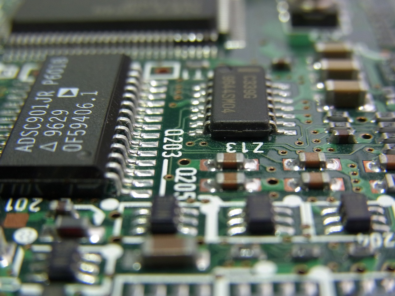
The process starts before the wafer enters the fab
Manufacturing begins with design intent, not with silicon. A chip architecture is converted into circuit layouts, verified through electronic design automation, and prepared as mask data. The completed layout is used to create photomasks or reticles, which transfer patterns onto wafers during lithography. Semiconductor Industry Association materials describe the value chain as moving from research and design into front-end manufacturing and then back-end manufacturing, rather than treating the fab as a stand-alone activity.
This matters because design rules define what the factory can reliably print and process. Minimum line widths, spacing, layer stack, transistor structure, power routing, test structures, and package requirements all influence manufacturing choices. A design may look efficient at the layout level but still be difficult to manufacture if it pushes lithography, overlay, thermal, or packaging limits too far.
Once the design is ready, wafers are prepared for production. Most mainstream integrated circuits are built on highly polished silicon wafers. The wafer provides both the mechanical platform and the semiconductor substrate. Modern high-volume logic and memory production commonly uses large wafers to increase die output per batch, but the wafer size, node, and tool set depend on the product type and the fab’s installed capacity.
Front-end wafer fabrication builds devices layer by layer
Front-end fabrication is the stage most often associated with chipmaking. It transforms a blank wafer into a patterned wafer containing many identical dies. The flow is not a simple linear recipe. Core unit processes are repeated many times, with metrology and inspection inserted throughout the line.
Film growth and deposition
Deposition adds thin layers of material to the wafer. These layers may be insulators, conductors, barrier films, hard masks, or semiconductor materials. Common approaches include chemical vapor deposition, physical vapor deposition, atomic layer deposition, and thermal oxidation, depending on the material and the required uniformity. The challenge is not only to place material on the wafer, but to control thickness, composition, stress, and defect performance across every die location.
Photolithography and pattern transfer
Photolithography defines where the next change will occur. A light-sensitive photoresist is applied, exposed through a mask pattern, and developed so selected regions remain protected while others are opened. ASML’s public technology materials describe lithography as a central step in chip production because it determines how circuit patterns are printed with high precision. Deep ultraviolet lithography remains widely used, while extreme ultraviolet lithography is used for some of the smallest and most demanding layers in advanced chips.
Lithography performance depends on resolution, overlay, focus control, mask quality, resist behavior, and tool stability. A small patterning error can change transistor behavior, contact resistance, leakage, or timing. For this reason, lithography is paired with extensive metrology rather than treated as a stand-alone exposure step.
Etching, doping, and material modification
Etching removes material from the regions opened by lithography. Wet etching uses chemical solutions, while dry plasma etching can provide more directional control for fine features. The goal is to remove the right material at the right rate without damaging nearby structures.
Doping changes the electrical properties of selected semiconductor regions. Ion implantation is commonly used to introduce controlled amounts of dopant atoms, followed by thermal steps that activate the dopants and repair crystal damage. Other modification steps may include annealing, silicidation, surface treatments, and cleaning. Together, these processes create the source, drain, channel, isolation, and contact regions that allow transistors to function.
CMP, cleaning, and defect control
Chemical mechanical planarization, often called CMP, flattens wafer surfaces after films are added or patterned. Without planarization, later lithography steps would have to work across uneven topography. Cleaning removes particles, residues, metals, and organic contamination between operations. These steps may be less visible than lithography, but they are essential for yield because a single particle can destroy a die or weaken long-term reliability.
Interconnect formation turns devices into circuits
After transistor formation, the process moves into interconnect construction. Transistors must be connected into functional logic blocks, memory arrays, analog circuits, or mixed-signal systems. This requires multiple metal layers separated by insulating dielectrics, with vias connecting one layer to another.
Interconnect manufacturing repeats deposition, lithography, etching, planarization, and cleaning. Lower metal layers usually handle dense local connections, while higher layers route longer signals and power distribution. As devices scale, interconnect performance can become a major constraint because resistance, capacitance, electromigration, and thermal behavior affect speed and reliability.
This is one reason process development is no longer only about shrinking transistor dimensions. Foundries and integrated device manufacturers must also improve materials, patterning methods, contact resistance, power delivery, and package-level integration. In practice, the integrated circuit manufacturing process now extends beyond the wafer into how dies communicate, dissipate heat, and integrate with memory or other chiplets.
Metrology, inspection, and yield learning run through the whole flow
Quality control in IC manufacturing is continuous. NIST publications on semiconductor metrology emphasize measurement needs across lithography, film thickness, surface inspection, interconnect materials, and process support. In a fab, metrology checks whether a process is hitting its target, while inspection looks for defects that may reduce yield.
Important measurements include critical dimension, overlay, film thickness, sheet resistance, defect density, wafer flatness, and electrical parameters from test structures. Some measurements are performed after key steps; others are sampled to avoid slowing the factory. Manufacturing teams use this data for statistical process control, excursion detection, tool matching, and yield improvement. See also: buying guides.
Yield is the share of good dies produced from a wafer. It is influenced by random defects, systematic design-process interactions, equipment drift, contamination, marginal patterning, and package-related failures. High yield is not simply a quality metric; it is an economic requirement. A process with strong device performance but poor yield can be too expensive for volume production.
| Control point | What it checks | Why it matters |
|---|---|---|
| Critical dimension metrology | Feature size after patterning or etch | Affects device speed, leakage, and matching |
| Overlay measurement | Alignment between layers | Prevents shorts, opens, and contact errors |
| Film thickness measurement | Uniformity of deposited or grown layers | Controls electrical and mechanical behavior |
| Defect inspection | Particles, pattern defects, scratches, residues | Supports yield learning and excursion control |
| Electrical test structures | Resistance, leakage, threshold behavior | Connects process results to circuit performance |
Wafer probe, dicing, and back-end manufacturing
When wafer fabrication is complete, the wafer still contains many connected dies. Wafer probe, also called wafer sort, electrically tests dies while they are still on the wafer. Intel’s public assembly and test materials describe wafer sort as an early test step that helps identify known good dies before packaging. This avoids spending package cost on dies that are already defective.
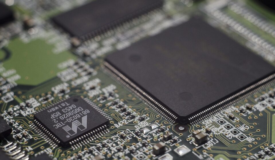
After probing, the wafer is diced into individual dies. Good dies are assembled into packages using steps such as die attach, wire bonding or flip-chip connection, underfill, molding or lid attach, marking, and singulation, depending on the package type. The Semiconductor Industry Association describes back-end manufacturing as the stage that turns fabricated wafers into ready-to-use chips through assembly, packaging, and testing.
Packaging has several roles. It protects the die from mechanical and environmental damage, provides electrical connections to a circuit board or module, helps remove heat, and supports handling in automated assembly. Traditional packages focused mainly on protection and connection. Advanced packages increasingly shape system performance by integrating multiple dies, high-bandwidth memory, interposers, bridges, or three-dimensional stacking.
Why advanced packaging is changing IC manufacturing
For many products, the boundary between manufacturing and packaging is becoming less clear. TSMC describes its 3DFabric family as including technologies such as SoIC, CoWoS, and InFO that support system-level integration of multiple chip components. Intel also describes advanced packaging and test technologies as important for systems made from multiple chiplets and components.
The manufacturing implication is significant. Instead of building every function on one large die, companies can combine chiplets made on different process nodes or optimized for different functions. A high-performance product may pair logic, memory, analog, I/O, and power-management components in one package. This approach can improve design flexibility, but it also adds process challenges: die-to-die alignment, warpage, thermal management, substrate supply, known-good-die strategy, and more complex final test.
Advanced packaging does not remove the need for precise wafer fabrication. It changes where value is created and where failures can occur. A defect in one chiplet, interposer, bump array, or assembly step can affect the entire package. As a result, test coverage, traceability, and process control must extend across both front-end and back-end operations.
A practical flow summary for IC production
The exact recipe differs by product, node, material system, and manufacturer, but a simplified integrated circuit manufacturing flow can be summarized as follows:
- Design and verification: Engineers define architecture, circuits, layout, timing, power, and manufacturability constraints.
- Mask preparation: Verified layout data is converted into masks or reticles used for lithography.
- Wafer preparation: Polished wafers enter the fab and are tracked through tightly controlled lots.
- Front-end fabrication: Deposition, lithography, etching, doping, CMP, cleaning, and inspection build transistors and isolation structures.
- Interconnect formation: Metal and dielectric layers connect devices into complete circuits.
- Wafer-level test: Probe testing identifies good and bad dies before packaging.
- Dicing and assembly: The wafer is cut, and good dies are attached and connected in packages.
- Final test and qualification: Packaged chips are electrically tested, screened, and prepared for shipment.
This sequence is useful as a learning model, but real fabs operate with rework rules, hold points, sampling plans, parallel tool groups, and product-specific modules. The main point is that IC manufacturing is an integrated system. A change in lithography can affect etch. A change in film stress can affect overlay. A package decision can affect wafer test strategy. Good manufacturing management therefore requires both step-level expertise and full-flow thinking.
Frequently asked questions
What is the most important step in the integrated circuit manufacturing process?
There is no single step that determines success for every chip, but lithography, etching, deposition, and metrology are among the most critical in wafer fabrication. Lithography defines the pattern, etching transfers it, deposition builds the material stack, and metrology verifies whether the process remains within control limits.
How is front-end manufacturing different from back-end manufacturing?
Front-end manufacturing builds the circuits on a wafer. Back-end manufacturing separates the dies, assembles them into packages, connects them electrically, and performs final testing. Both stages affect yield and reliability, but they use different equipment, materials, and process controls.
Why are chips tested more than once?
Testing at several points reduces cost and improves reliability. Wafer probe can identify defective dies before packaging. Final test checks the packaged device under defined electrical conditions. Advanced packages may need additional test steps because multiple dies and interconnect paths must work together.
Does advanced packaging replace transistor scaling?
No. Advanced packaging complements transistor scaling. It allows manufacturers to combine different dies or chiplets more efficiently, but high-performance logic, memory, and analog functions still depend on strong wafer fabrication processes.
Why is yield so important in IC manufacturing?
Yield determines how many sellable chips come from each wafer or package build. Because semiconductor tools, cleanrooms, masks, substrates, and process time are expensive, even small yield changes can strongly affect unit cost, capacity planning, and delivery reliability.